 |
| May 11, 2021 | Volume 17 Issue 18 |
Designfax weekly eMagazine

Archives
Partners
Manufacturing Center
Product Spotlight
Modern Applications News
Metalworking Ideas For
Today's Job Shops
Tooling and Production
Strategies for large
metalworking plants
50 billion transistors on a chip the size of a fingernail: IBM unveils world's first 2-nm chip
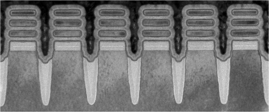
Row of 2-nm nanosheet devices. [Credit: IBM]
IBM has just announced a breakthrough in semiconductor design with its creation of the world's first chip with 2-nanometer (nm) nanosheet technology. Developed less than four years after IBM announced its milestone 5-nm design, this latest 2-nm breakthrough means up to 50 billion transistors can fit on a chip the size of a fingernail.
Semiconductors play critical roles in everything from computing to appliances to communication devices, transportation systems, and critical infrastructure. More transistors on a chip also means processor designers have more options to infuse core-level innovations to improve capabilities for leading-edge workloads like AI and cloud computing, as well as new pathways for hardware-enforced security and encryption.
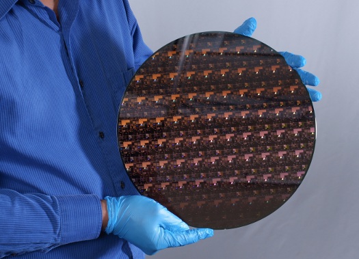
IBM's chips are fabricated on large wafers. Each wafer contains hundreds of chips the size of a fingernail, each with 50 billion 2-nm transistors. [Credit: IBM]
Demand for increased chip performance and energy efficiency continues to rise, especially in the era of hybrid cloud, AI, and the Internet of Things. IBM's new 2-nm chip technology -- which features components that are smaller than a strand of DNA -- helps advance the state-of-the-art in the semiconductor industry, addressing this growing demand. It is projected to achieve 45% higher performance, or 75% lower energy use, than today's most advanced 7-nm node chips.
IBM is pretty optimistic about the long-term potential of these advanced 2-nm chips, projecting benefits that could include:
- Quadrupling cell phone battery life, only requiring users to charge their devices every four days.
- Slashing the carbon footprint of data centers, which account for 1% of global energy use.
- Drastically speeding up a laptop's functions, ranging from quicker processing in applications to assisting in language translation more easily and faster internet access.
- Contributing to faster object detection and reaction time in autonomous vehicles like self-driving cars.
This latest breakthrough builds on decades of IBM leadership in semiconductor innovation. The company's semiconductor development efforts are based at its research lab located at the Albany Nanotech Complex in Albany, NY, where IBM scientists work in close collaboration with public and private sector partners to push the boundaries of logic scaling and semiconductor capabilities.
IBM's first commercialized offering if its 7-nm advancements will debut later this year in IBM POWER10-based IBM Power Systems.
Source: IBM
Published May 2021
Rate this article
View our terms of use and privacy policy